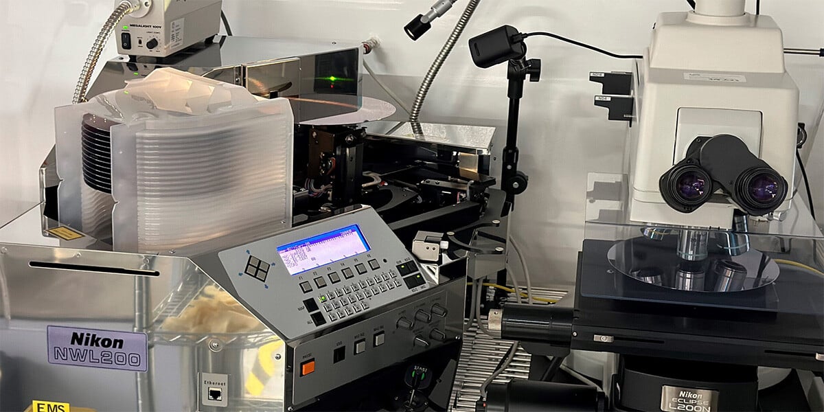
Lawrence Semiconductor has partnered with Nikon Metrology to upgrade its wafer inspection processes. By integrating Nikon’s NWL 200 wafer loader system with the Eclipse L200 microscope, we've achieved faster throughput and improved inspection accuracy, allowing for 100-percent inspection of wafer lots.
This advanced solution supports our mission to provide high-quality, innovative semiconductor technology.
Our CEO, Ali Torabi, emphasizes the importance of this partnership: "Our collaboration with Nikon is instrumental in supporting our current and future inspection requirements, ensuring we maintain our reputation for excellence in semiconductor technology."
To learn more about this partnership and its impact, visit Nikon’s press release.