EPITAXIAL WAFER SERVICES
Epitaxy is the key enabling technology for today’s high performance semiconductor devices. We offer a comprehensive portfolio of Silicon epitaxy processes and characterization capabilities.
CUSTOM EPITAXY SOLUTIONS
Our epitaxy services enable a wide range of customer device applications, including Silicon Photonics, Power Devices and PIN Diodes, MEMS, Quantum Computing, Virtual Substrates, CMOS Logic, and Specialized Detectors
Our process capabilities include:
- Selective and blanket epitaxial growth of silicon (Si), germanium (Ge), silicon-germanium (SiGe), carbon-doped silicon-germanium (SiGe:C), germanium-tin (GeSn), and silicon-germanium-tin (SiGeSn) and low defect density SiGe and Ge epitaxial structures for short and mid wave infrared (SWIR and MWIR) photodetectors and imagers
- SiGe on Si and SiGe on Ge quantum well structures for optical modulators and quantum computing
- Si-28 growth for spin qubit-based quantum computing
- Strained Si:C or SiGe or Si:P layers on silicon or SOI for enhanced mobility FETs
- Thick silicon PIN diodes for power devices
- Controlled doping profiles with abrupt or graded transition for PIN diodes and other devices with carrier concentration control ranging from 5E+13 to >1E20/cm3
- Pure Boron on n-Si to form ultra shallow p+/n junctions for UV detectors
- Virtual substrates with abrupt single composition, Thick Graded Buffers (TGB), Reversed Graded Buffers (RGB)
- Poly- and mono-crystalline silicon on insulator or SOI for MEMS devices with thickness ranging from 1µm to 500µm
- Conformal poly silicon fill of high aspect ratio through silicon vias (TSVs)
- Epitaxial growth over patterned buried layers with optimized pattern integrity and autodoping control


CHARACTERIZATION
- FTIR and Spectroscopic Ellipsometer for epi thickness
- Four-point probe for sheet resistance (CDE Resmap)
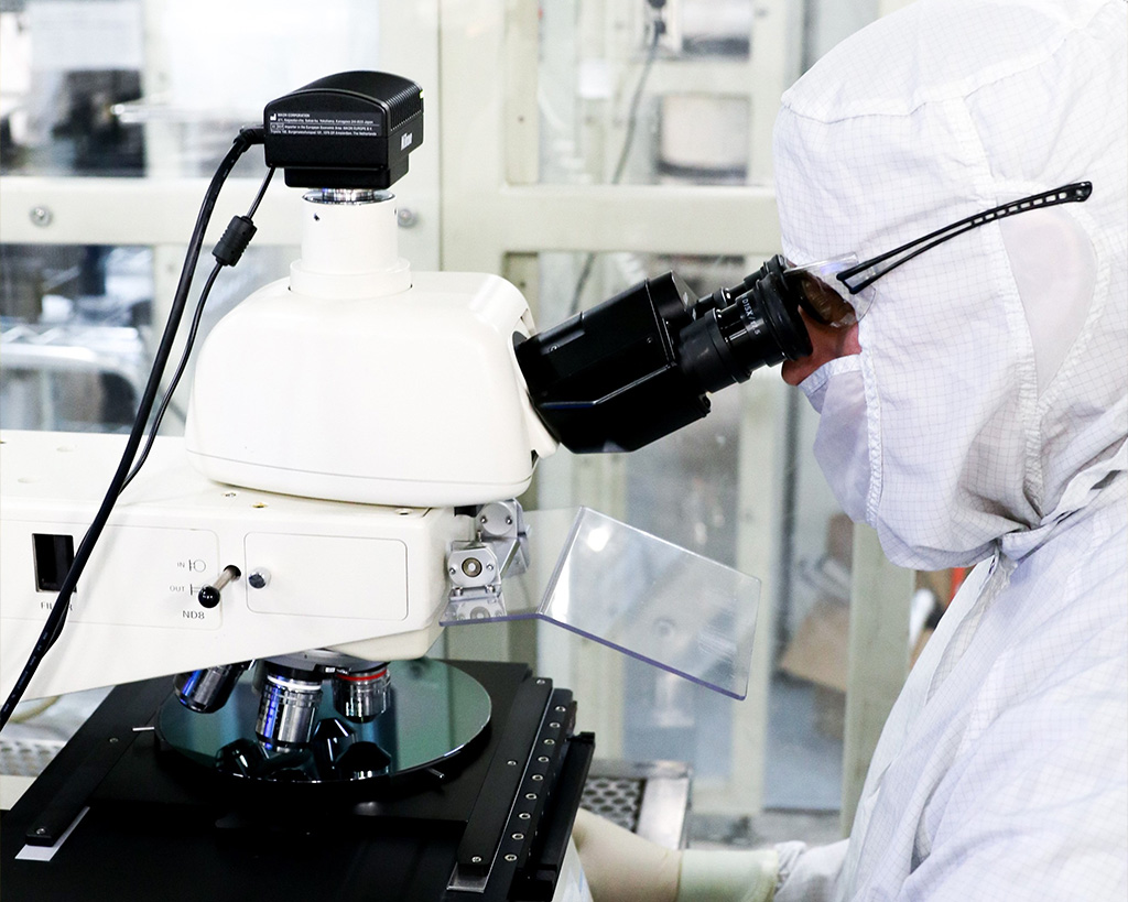
- Optical microscopes with Nomarski interference contrast (Nikon Optiphot)
- Bright-light for wafer inspection
- Tencor Surfscan for particles and haze mapping
- Wafer bow and warp gauge (ADE 9500)
- Spreading Resistance Probe (SSM 150) for depth profiling of carriers, thickness, and junction characterization
- Atomic Force Microscopy (AFM) for film surface roughness and step-height measurements
- Room temperature and 4K PL up to 5um
- Membership access to a wide variety of materials characterization services at Arizona State University’s Leyroy Eyring Center for Solid State Science, including XRD, FiB SEM and EDX, TEM, Raman Spectroscopy, RBS, Auger, XPS, and CL
- SIMS (Quadrupole and Magnetic sector) by EAG
- VPD-ICP MS for surface contaminants by Chemtrace
OPERATIONS:
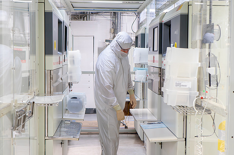
- 15,500 sq. ft. facility in Tempe, Arizona
- Class 10 clean room
- 24/7/365 operation
- 15 optimized epitaxial reactors capable of operating at reduced and atmospheric pressures” with “Chemical vapor deposition (CVD) reactors capable of operating at reduced and atmospheric pressures
- Single and multi-wafer epi production on wafers up to 200mm diameter
- High yields (>99.5%)
- ISO 9001:2015 Quality Management System Certified
- Manufacturing Execution System
- Extensive quality management system with statistical process controls, failure mode and effects analysis, and internal audits
